Overview
This research applied a structured measurement and analysis methodology to quantify power optimization trade-offs in nanoscale circuits. By systematically varying layout configurations and measuring energy per operation across each variant, the study produced empirical data to guide design decisions — a methodology directly analogous to performance profiling and benchmarking in software engineering.
Research Focus
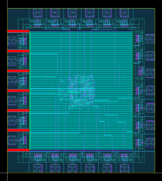
This project studies the effects of multi-finger transistor layout on energy and power consumption in asynchronous circuits. Multi-finger layout splits a single wide transistor into multiple narrower fingers connected in parallel, which can reduce parasitic capacitance and improve switching characteristics.
Null Convention Logic (NCL) — a delay-insensitive asynchronous design technique — was used as the target design style, implementing a full adder in various multi-finger configurations.
Methodology
- Designed NCL full adder cells in multiple multi-finger configurations
- Used Cadence Virtuoso for schematic capture and layout
- Performed power estimations using Cadence power analysis tools
- Simulated waveforms using Virtuoso waveform analysis
- Compared configurations across energy per operation and peak power draw
Results
The data shows measurable advantages of different multi-finger configurations for an NCL full adder circuit. Specific configurations achieved reduced dynamic power at the cost of increased layout area, while others balanced area and power efficiently.